
The work is licensed under
a Creative
Commons Attribution-NonCommercial-ShareAlike 4.0 International
License.
2023-03-23
The work is licensed under
a Creative
Commons Attribution-NonCommercial-ShareAlike 4.0 International
License.
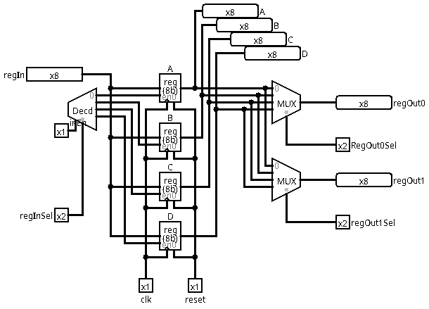
The register bank (sub-circuit regBank) houses four
software addressable registers. This means these four
registers, labeled register A to register D in TTPASM, can be specified
explicitly in opcodes. The register bank can update one of the four
registers, and connect up to two of the registers to the output of the
register bank.
Look into the regBank circuit, and understand how it
operates. Specifically, figure out the following:
regBank. There are two outputs.ALU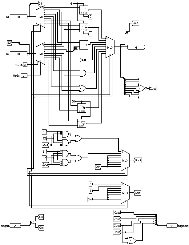
The ALU (arithmetic and logic unit) is responsible for
computations and “logic.” Logic, in this case, is merely determining
some elementary conditions, such as whether the minuend is less than the
subtrahend in a subtraction, or whether the result of an operation is
zero.
The ALU itself does not provide values to computations,
nor does it store the results of computations. In TTP, registers are
used to supply data for computations, as well as to store results of
computations.
In the circuit of the ALU, there are many multiplexers
and demultiplexers to route values needed for computations and results
from computations. Track down how this routing is specified by the input
pins of the ALU. Furthermore, track down the outputs of the
ALU, and backtrack to figure out what each output
represents. This is particularly important for the bits related to
flagsIn and flagsOut.
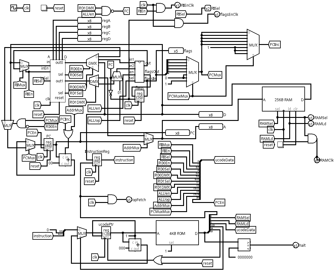
The controller is the lower portion in the TTP, centering around the only ROM component.
The controller is responsible for the coordination of all the other parts of TTP to perform actual operations.
Technically, the RAM component is not a part of TTP. In reality, RAM is often outside of the die of a processor because it takes up more spaces. However, the are processor chips that include RAM when the amount of RAM can be combined to the same die.
RAM is used to store/supply opcodes, this is the main idea of a von Neumann architecture. However, RAM is also used to store global variables, as well as the stack.
TTP has a few registers that are not software addressable. This means that these registers cannot be directly accessed by opcodes.
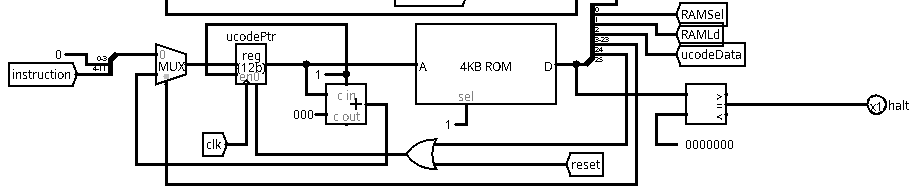
ucodePtr: the microcode pointer is a register that
connects to the ROM component. This register is at the core of
controller part of TTP. Of all the registers, ucodePtr is
the only one that is sensitive to a falling edge instead of a rising
edge.PC: the program counter stores the address in RAM (not
ROM) of where to find the next opcode.flags: the flags register stores the carry, zero,
overflow, sign, and less-than flags from the ALU from the most recent
ALU operation. These flags can, then, be utilized by conditional branch
instructions.InstructionReg: the instruction register temporarily
stores a copy of the opcode in RAM that is pointed to by
PC, which is then used to update ucodePtr to
“decode” an opcode.At first glance, TTP looks like a big mess with wires and tunnels everywhere. However, there is a structure method to gain an understanding of how it gets work done.
When ucodePtr==0 on a rising edge,
InstructionReg=*PC, and this is called the fetch
cycle/phase of executing an opcode. You may want to examine location 0
of the ROM, and see how registers are enabled, how RAM is enabled, and
how multiplexers and demultiplexers are configured to accomplish the RTL
(register transfer language) description
InstructionReg=*PC.
Sort of part of the fetch cycle, when
ucodePtr==1 on a rising edge, PC=PC+1 to
autoincrement the program counter for the next opcode. Again, it is
useful to understand how the D port of ROM controls a multiplexer to
specify this behavior.
When ucodePtr==1 on a falling edge,
ucodePtr=InstructionReg << 4. Track down the circuit
to find out how this is accomplished by a splitter, a multiplexer, and
the corresponding bits from the D port of ROM.
After decode, ucodePtr points to a specific location in
ROM. The content at this location of ROM is presented to the D port of
ROM.
There is no easy way to describe what happens in the execute
cycle/phase of executing an opcode because this part depends on the
opcode. The ROM allocates 16 microcode slices (locations in ROM) per
opcode. However, most opcodes can be accomplished by two microcode
slices. Every opcode needs the last microcode slice to reset
ucodePtr to zero.
To analyze a specific microcode slice of a specific opcode:
regBank, ALU,
PC, RAM. These components have specific ports
that can help indicate whether they are in use or not.In simpler terms, to understand what a microcode slice does, first determine the active components used, then find out how these components are routed to each other.